SCREEN Joins IBM Sub-1nm Chip Technology Program
Kyoto-based SCREEN Semiconductor Solutions will co-develop advanced manufacturing processes and equipment for IBM's world-first sub-1nm chip technology, including High NA EUV lithography tools.
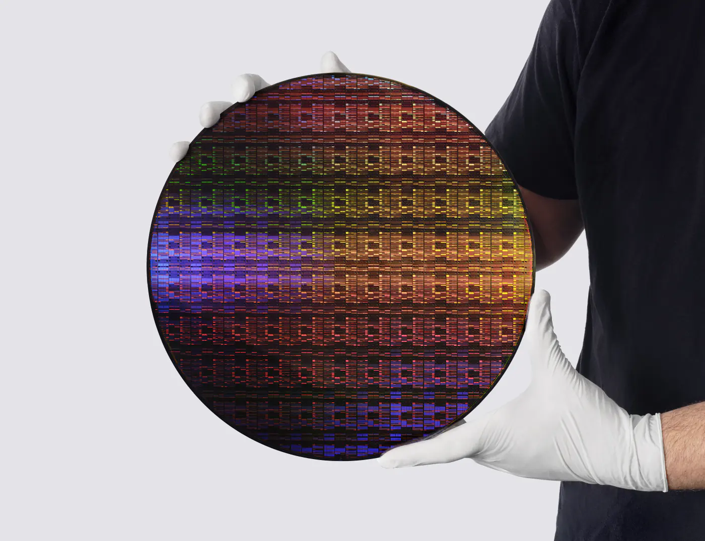
KYOTO — SCREEN Semiconductor Solutions, the Kyoto-based semiconductor equipment maker, announced July 9 it has joined IBM’s development program for the world’s first sub-1nm chip technology, disclosed by IBM on June 25.
SCREEN will collaborate on advanced manufacturing processes and equipment for production nodes below one nanometer, including tools for High NA extreme ultraviolet lithography. The company’s brief release names no other partners and discloses no financial terms.
Why it matters: The partnership positions a Kansai equipment supplier in the next wave of lithography tooling as chipmakers push toward sub-nanometer geometries. SCREEN’s participation signals its technological reach in cleaning and coating processes critical to High NA EUV, where tighter tolerances require new hardware approaches. IBM has not announced a timeline for commercial production.