SCREEN Launches Sub-micron Direct-write Lithography Tool for AI Chip Packaging
Kyoto-based SCREEN Semiconductor Solutions released the DW-3100, a maskless exposure system achieving resolution below 1µm for advanced packaging and heterogeneous integration.
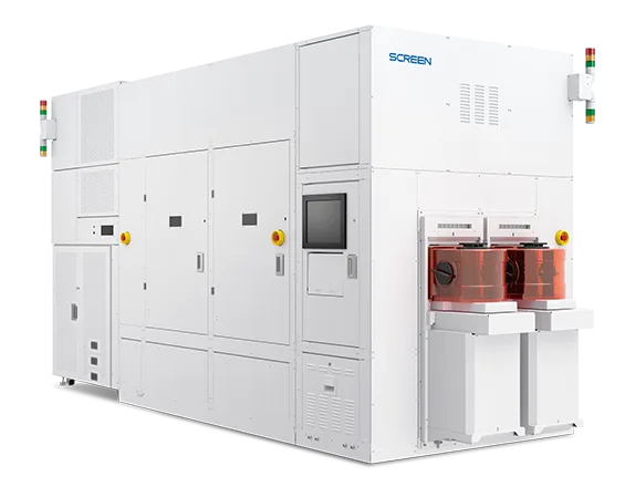
KYOTO — SCREEN Semiconductor Solutions released the DW-3100 direct-write lithography system this month, achieving sub-1µm resolution for advanced semiconductor packaging driven by AI chip complexity.
The tool uses SCREEN’s proprietary GLV (Grating Light Valve) technology — a MEMS-based light modulator controlling thousands of micro-ribbons simultaneously — to enable maskless exposure. The new model upgrades the optical system from the prior DW-3000, reaching resolution below one micron. On-board image processing compensates for wafer warpage, distortion, and chip misalignment, enabling optimized exposure per die. The system also handles rectangular panels in addition to round wafers.
Key capabilities
- Sub-1µm resolution via upgraded optics and GLV modulation
- Die-level distortion correction for heterogeneous integration workflows
- Unique ID patterning per chip for traceability in medical and high-reliability applications
- Panel format support alongside standard wafers
Why it matters: Maskless lithography eliminates reticle costs and turnaround delays, appealing to packaging houses dealing with rapid AI chip design cycles and mixed-die assemblies. Sales begin this month; SCREEN has not disclosed pricing or volume targets.