Panasonic Unit Launches On-site Copper Recovery Systems for Semiconductor Fabs
Osaka-based Panasonic Environmental Engineering enters semiconductor wastewater treatment market with compact metal recovery units, targeting cost reduction and resource recycling at smaller fabrication plants.
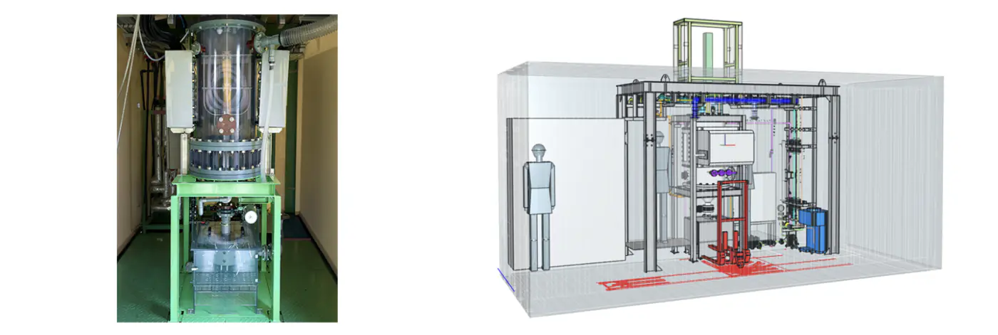
OSAKA — Panasonic Environmental Engineering, an Osaka-based subsidiary of Panasonic HVAC & CC, launched a wastewater treatment and metal recovery business for semiconductor and electronics factories, with unit-type copper recovery systems beginning sales in April 2026.
The core offering is RARELOOP, a packaged electrolysis system that extracts reusable copper from etching wastewater on-site. Unlike traditional large-scale plant systems, the compact units fit within limited factory floor space and lower upfront installation and maintenance costs. Recovered copper can be sold as a commodity, converting disposal expense into revenue. The company plans to extend the technology to silver, tin, and nickel.
The business covers three areas
- Metal recovery: RARELOOP units for copper extraction from etching waste
- Wastewater processing: Proprietary coagulation and decomposition methods for difficult-to-treat slurries and organic nitrogen compounds, reducing chemical use and equipment footprint
- Chemical supply: Low-temperature, long-life resist stripping agents for backend packaging processes, plus copper plating processes for glass substrates in next-generation semiconductor packages
Why it matters: Distributed recycling infrastructure reduces barriers for smaller facilities and lowers hazardous waste disposal costs — key considerations as semiconductor fab expansion accelerates globally.