Nikon Commercializes Advanced Wafer Alignment System Following NEDO-funded R&D
Nikon began taking orders for the Litho Booster 1000 alignment station, achieving 35% better measurement accuracy and 10% higher throughput than prior models, following a 2021–2025 NEDO development program.
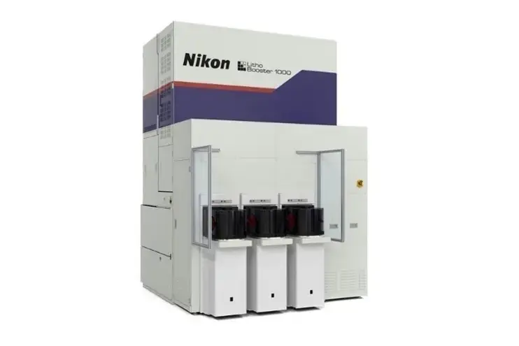
TOKYO — Nikon began taking orders for the Litho Booster 1000 alignment station, a wafer positioning tool delivering 35% improved measurement accuracy and 10% higher throughput over previous models, following R&D funded by Japan’s New Energy and Industrial Technology Development Organization (NEDO) from 2021 to 2025.
The system addresses a core challenge in advanced semiconductor manufacturing: measuring wafer position and distortion with high precision as devices shrink and manufacturers adopt 3D chip stacking. Traditional methods struggle when alignment marks are buried under opaque carbon hardmasks or multiple silicon layers. Nikon developed a new optical system suppressing chromatic aberration across visible and near-infrared wavelengths, paired with a high-output wideband light source, enabling detection of fine-pitch marks and marks beneath thick silicon films. NEDO verification confirmed the integrated system met specifications for accuracy, repeatability, and throughput under production conditions.
The Litho Booster 1000 incorporates some of the R&D results but not all of them. Nikon stated it will monitor customer needs and consider deploying additional technologies in future models.
Alignment precision directly impacts yield in sub-3nm nodes and 3D integration, where electrode pitch and layer count are rising. Japan-made metrology tools remain strategic as fabs seek resilient supply chains for critical process control equipment.