Rapidus Clears FY2026 Hurdle as Japan's 2nm Programme Moves Toward Production
Japan's NEDO has approved Rapidus' fiscal 2026 plan and budget for its 2nm front-end and advanced packaging projects. The decision lets the company move from pilot-line proof points toward yield improvement, broader design access and fuller back-end operations ahead of its 2027 mass-production target.
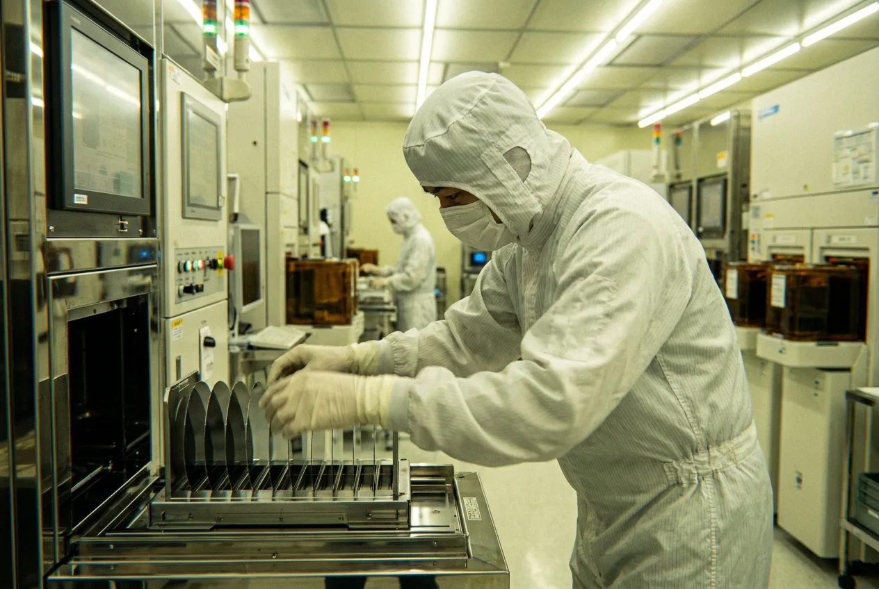
NEDO approves Rapidus FY2026 plan for 2nm chip projects
TOKYO — Rapidus has received approval from Japan’s state technology agency for its fiscal 2026 plans and budget, a routine but consequential step that allows the company to move its 2nm programme from early milestones into the harder, more expensive work of improving yield and preparing manufacturing systems for paying customers.
The New Energy and Industrial Technology Development Organization approved two separate projects under its post-5G semiconductor initiative. One funds front-end logic development, the process of fabricating 2nm transistors on silicon wafers using gate-all-around architecture, through a Japan–US research collaboration that has been running since November 2022. The other, launched in March 2024, covers the back-end side: chiplet integration, advanced packaging, and the design and test tools that customers need to deploy complex multi-die chips.
What FY2025 Produced
The significance of the FY2026 approval depends partly on what FY2025 actually delivered. At its IIM-1 foundry in Chitose, Hokkaido, Rapidus brought its pilot line online in April 2025, connecting over 200 pieces of advanced equipment inside a completed cleanroom. Engineers subsequently verified that 2nm gate-all-around transistors were operating correctly on 300mm wafers, the first time such a result had been confirmed in Japan. The company also issued a pre-release process design kit to a limited group of early-adopter customers, establishing a working environment for prototype chip design.
On the packaging side, the Rapidus Chiplet Solutions unit, operating from a facility at the Seiko Epson plant in Chitose, began installing back-end equipment in April 2025 and produced a prototype of an organic insulating-film redistribution-layer interposer on a 600mm square panel. Rapidus described the format as an industry first; the 600mm panel format is intended to raise interposer throughput by roughly ten times compared with conventional 300mm wafer-based processing, a potential cost and scale advantage for AI and high-performance computing chip packages.
What Changes in FY2026
With the new budget in place, Rapidus will move from limited pre-release access to a general PDK release, opening its prototype environment to a broader set of customers. The company will also validate the equipment, transport, and production management systems that underpin its short-turnaround-time model, the ability to complete prototype and low-volume runs faster than larger foundries typically accommodate.
CEO Atsuyoshi Koike said the company would focus on improving prototype accuracy and implementing yield improvement measures on the wafer side, while advancing 2.xD and 3D packaging manufacturing on the back end. “With the approval of the NEDO project plan and budget, in the wafer process, we will further improve the accuracy of prototypes and implement measures to increase yield,” Koike said. “For the chiplet area, we will continue to advance the development of 2.xD and 3D packaging manufacturing technologies, including those for 2nm-generation semiconductors, with the aim of steadily progressing toward the start of mass production targeted for 2027.”
Rapidus was founded in August 2022 and holds capital of 274.95 billion yen as of February 2026. Mass production of 2nm wafers is targeted for the second half of fiscal year 2027.